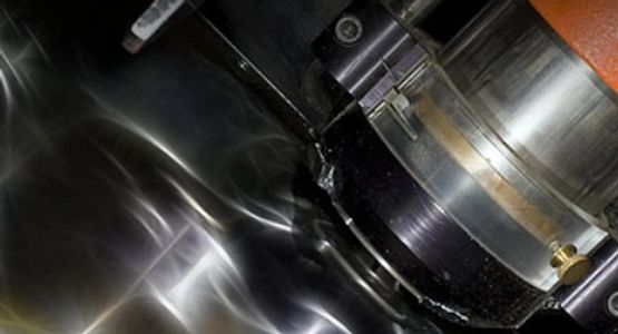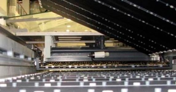
Front End
Front End is the term used to describe what is essentially the start of the PCB manufacturing process. It’s here that a customer’s files will arrive and it’s then down to us to manipulate these files into the various formats used in printed circuit board manufacture.
The engineers will perform a very detailed DRC of the customer's data, ensuring that the data can be manufactured and also that the designer has not made any errors.
For example, with a typical Plated Through-Hole (PTH) PCB, the customer will supply us with files showing the 2 copper layers (usually labelled TOP & BOTTOM…but not always!), 2 Solder Resist layers, 1 or maybe 2 Ident layers, drilling co-ordinates, and a board outline drawing.
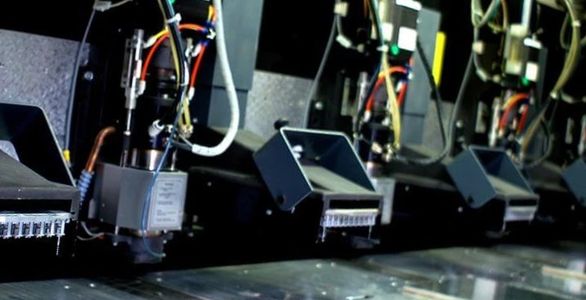
The Laser Photo-plotter exposes each layer of the circuits onto a piece of clear film. The film is then developed and is ready for use.
One Way PCB can accept many different formats of data. Most data is received in Gerber format via email.
See our Front end design rule checker for help with PCB design.

Drilling
To set up the drill, the operator first puts a panel of exit material on the drill bed. This stops the drill tearing the copper foil as it comes through the PCB. They then load one or more PCB panels, and a sheet of aluminium entry foil.
The drilling machine is computer-controlled. The operator selects the right drill program. This tells the machine which drill to use and the XY co-ordinates of the holes. These drills use air-driven spindles which can rotate up to 150,000 RPM. High speed drilling ensures clean holes to provide a secure base for good plating on the hole walls.
Drilling is a slow process as each hole must be drilled individually. So depending on the drill size we drill a stack of one to three PCB panels together. We can drill holes down to 100 microns in diameter. To give you an idea of the size, a human hair has a diameter of about 150 microns. Drill change is fully automatic. The machine selects the drill to use from the drill rack, checks that it is the correct size, and then loads it into the drill head.
Once all the holes are drilled the operator unloads the panels from the drilling machine and discards the entry and exit material.
All the drilling machines are connected to the network allowing quick updating of the drill files. Automatic loaders and un-loaders enable the machines to run overnight unsupervised.

Direct Metalization
Direct metalization is a highly stable graphite based system for use with horizontal flood conveyorized process equipment. The full process sequence is comprised of three chemical stages.
The process is used to place a small amount of graphite down the holes of panels, which need a connection between the top and bottom layers, i.e. PTH and Multilayer.
The panels pass through a cleaner then into a rinse before going into the graphite chamber. The panels are completely submerged in graphite and when they come out of the chamber the whole panel has a thin coating of graphite on it.
The panels then go through an oven to bake the solution onto the panel. As we only require the graphite down the holes for plating, it is no longer needed on the surface so the panels pass into a micro-etch chamber which removes the graphite from the surface. This restores the clean copper surface while leaving the graphite coating in the holes.
The whole process takes about seven minutes.

Photomech room
All panels are taken into the Photo-mech for the image of the tracks to be created onto them.
Before this can take place the panels are lightly surface cleaned and then laminated with ultra violet light sensitive dry-film.
The films that were produced by the Front End department are then aligned onto the panels and the panels are then placed into an exposure unit. The exposure unit uses ultraviolet (UV) lights to expose the image on the artwork onto the dry film. This is the same process for single sided / PTH or Multilayer.
The panels are placed through a conveyed machine which, using a chemical solution, develops to wash the areas of dry film from the panels that we do not require, leaving just the image of the artwork on the panels.

Plating
Copper tanks are used to plate the required amount of copper both down the holes and onto the surface of the panels.
As the process is electrolytic, the panels are placed onto jigs, which are then placed into the rober bar above the solution. An electric current is passed through the jigs and onto the panels from a power supply. The higher the current, the more negative copper solution is then plated onto the boards.
The amount of current required is calculated by the amount of copper area exposed to be plated, this calculation ensures that the panels are plated to the correct thickness. We always plate between 25-35 microns for a standard 1oz finish.10-15 microns of Tin is then plated over the top of the copper in exactly the same way to protect the copper when the panel are etched.
This process takes about 80 mins from pre-clean to end.

Etching
PCB etching process is one of the major steps in the chemical processing of subtractive printed circuit board. It is the removal of copper, to achieve the desired circuit patterns. In PCB etching process, all copper is removed except the circuitry that is protected by the tin plating applied during the previous treatment in PCB manufacture. The tin is then stripped and the copper is cleaned and the newly prepared circuit is ready for solder mask.
After this process the panels are left with only the copper track - and this is where they actually begin to look like PCBs.

Solder Resist
The manufacturing panels pass through the ink curtain at a typical speed of 90 m/min. The ink is automatically pumped into the coating head from the supply container. A microprocessor-aided viscosity control in the ink container ensures a precise viscosity of the ink, by automatically adding solvents and permanent temperature control.
The coating head produces a vertically falling ink curtain. The PCBs are coated in the desired layer thickness in an extremely homogeneous way
The panels then go through the Infrared (IR) oven until they are part cured. At this stage, the solder resist artwork is used. The boards are exposed again, which creates the image of the solder resist pattern on the panels.
Finally, the panels are 'cured' in an oven at 150 degrees for around 50-70 minutes depending on thickness.

Surface Finish
A PCB surface finish is a coating between a component and a bare board PCB. It is applied for two basic reasons: to ensure solderability, and to protect exposed copper circuitry. We can offer the following:
Lead-free HASL
Lead-free HASL is a ROHS compliant finish – it has been developed as a lead-free alternative to the traditional Leaded HASL finish. It is applied by solder dipping the PCB followed by removal of excess solder by blowing with air-knives to produce a flat solder finish.
OSP (Organic Solderability Preservative)
OSP is a RoHS compliant finish. It is an anti-oxidant film applied to the exposed copper surface. It reacts with the copper to form an organo-metallic layer, the coating is virtually invisible.
Emmersion Silver
Immersion silver is a RoHS compliant finish. It is produced by the selective displacement of the copper atoms by silver atoms on the exposed copper surface. It is compatible with surface mount, BGA and through hole components.
Electroless Nickel Immersion (ENIG)
ENIG is a RoHS compliant finish. It is applied through the deposition of an initial layer of Nickel onto the copper surface, followed by a thin protective layer of gold, Nickel characteristics of hardness, wear resistance, solderability and uniformity of deposition makes this an excellent surface finish. The thin layer of gold preserves the solderability of the finish by preventing oxidisation of the highly active nickel surface. It is compatible with surface mount, BGA and through hole components.

PCB Ident
Conventional silk-screening requires polyester screens stretched across aluminium frames. Solvent resistant emulsions are used to coat the screens prior to imaging. Both the screen and panel must be registered precisely to ensure proper alignment. This method of screening requires the following equipment: Laser photo plotter to produce the initial film, UV printer, spray developer and curing ovens.
.jpg/:/cr=t:16.59%25,l:0%25,w:100%25,h:76.92%25/rs=w:600,h:300,cg:true)
Testing/Inspection
The flying probe test (FPT) is an electrical test method, which makes a simultaneous in-circuit test (ICT) of the top and bottom of a module easily and flexibly.
6 high-precision probes (needles), 4 on top and 2 on the bottom, are programmatically able to contact component pins (including fine-pitch components) or other contact points on a printed circuit board or assembly to perform an electrical test.

Profiling
The last stage is to rout and score.
CNC routing machines use the data from Front End to profile your boards to the correct size and shape, using small cutting tools which move along the profile.
One Way PCB can also supply scored panels, boards can be provided within a scored panel so they can be snapped out easily, after assembly.
Contact Us
One Way PCB
Units 1, 2 & 3 Halifax Court, 50 Hurricane Way, Norwich, NR6 6JB
Hours
Open today | 09:00 – 17:00 |